Please wait...

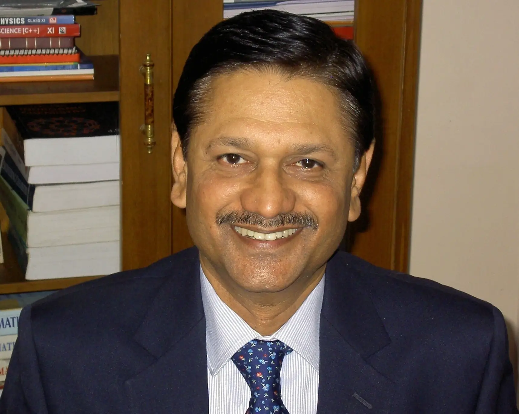
Faculty details Rajiv O. Dusane
Institute Chair Professor

Rajiv O. Dusane

Email: rodusane[at]iitb[dot]ac[dot]in

Phone: (+91) (022) 2576 7633

Education: 

  • Ph.D. ­ Physics, 1990, Univ. of Poona, Pune, 
  • M.Sc. ­ Physics, Nagpur Univ ­ 1984
Teaching

Prof. Dusane has engaged students in thin films and semiconductor device processing courses over the last 20 or more years with special emphasis on the practical aspects. He also established the Thin Film lab for both UG and PG students. As his special interest he also took the communication course for the PG students. 

Undergraduate course: Science and Technology of Thin Films 

Postgraduate course: Materials and Processes for Semiconductor Device Manufacturing

Research profile

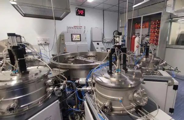
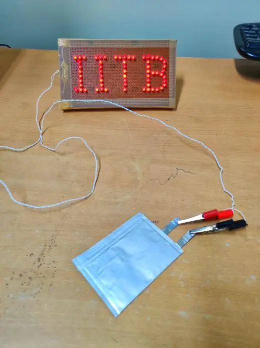
Prof. Dusane has over the last 30 years carried out fundamental and applied research in the area of semiconductor thin films and devices, surface modification and plasma processing of various materials with a view to develop new processes and materials in thin film and nano structure form, capable for a variety of applications ranging from solar cells, thin film light emitting devices (TFLEDs), microelectronic devices, sensors and actuators (MEMS) and batteries. He has done pioneering work in the area of Hot Wire Chemical Vapor Deposition (HWCVD) process in this country. Several patents have resulted out of this work and some successful industrial collaborations have also been undertaken. Over these years he has established state of the art facilities for thin film deposition and characterization. Recent significant work from his group is the Silicon nanowire­based anode for Li­ion battery. The work carried out till now has demonstrated the capabilities of the Hot Wire process in diverse areas like Microelectronics, Biocompatible materials, surface functionalization and modification, barrier layers etc. This has given new directions to the applicability of the HWCVD process in the area of MEMS and sensors. Recently he has designed and developed a HWCVD multi­chamber cluster tool, the first of its kind in the country.

Research interest
  • Semiconductor thin films for optoelectronic devices, 
  • Photovoltaic devices, 
  • Energy storage

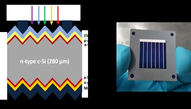
HIT solar cell on textured Silicon wafer architecture and fabricated cell

The newly developed HWCVD multichamber system

Silicon Nanowire Anode based Li­ ion pouch cell

References
  1. Rashmi Tripathi, V Chauhan, P Gandharapu, S Kobi, A Mukhopadhyay, R O Dusane. “Si Nanowires Grown on Cu Substrates via the Hot­Wire­ Assisted Vapor–Liquid–Solid Method for Use as Anodes for Li­Ion Batteries”. ACS Applied Nano Materials (2022), 17767–17782. 
  2. "Conformal Deposition of BxC in High Aspect Ratio Trenches for 3­D neutron detectors", Gourav Kumar, Partha Karar, D S Patil, Arvind Singh, Anita Topkar, R O Dusane Thin Solid Films 720 (2021) 138521 
  3. "Piezoresistive pressure sensor using nanocrystalline silicon thin film on flexible substrate", V Pandey, A Mandal, S Sisle, MP Gururajan, R O Dusane Sensors and Actuators A: Physical 316, 112372

Faculty Details Avradeep Pal

Associate Professor

Avradeep Pal

Email: avradeep[at]iitb[dot]ac[dot]in

Phone: (+91) (022) 2576 7629

Education: 

  • PhD ­ Materials Science, University of Cambridge, 2014 
  • M. Tech ­ Materials Science, IIT Bombay, 2010 
  • B. Tech ­ Metallurgy and Materials Science, 2006
Teaching

In his teaching, Avradeep focuses primarily on conceptual understanding of origin of physical phenomena, with a special attention to stay clear of rote memorisation as much as possible. Courses taught: Undergraduate ­ Structure of Materials Post Graduate ­ Advanced Ceramics (Piezoelectrics, Ferromagnets, Superconductors)

Research profile

Avradeep's interests lie in the sphere of development, understanding and utilisation of novel phenomena that arises at hybrid material interfaces, and development of several novel quantum devices. The major focus is on the interface of thin film superconductors and ferromagnets. His work therefore spans from controlled Ultra High Vacuum growth of ultra thin film (2nm and lower) multi­layers, to nanofabrication of these layers into devices like tunnel junctions, spin valves, Jospehson junctions; and subsequent low temperature electronic transport measurements of such devices. For achieving the same, he has developed several highly customised UHV thin film deposition and fabrication systems, and has standardised a industry level niobium based junction fabrication process. This has led to the discovery of novel cryogenic memory devices and other cryogenic components such as Josephson diodes that are crucial for upcoming era of quantum technologies.

Research interest
  • Superconducting devices, 
  • Josephson effect, 
  • Superconducting spintronics

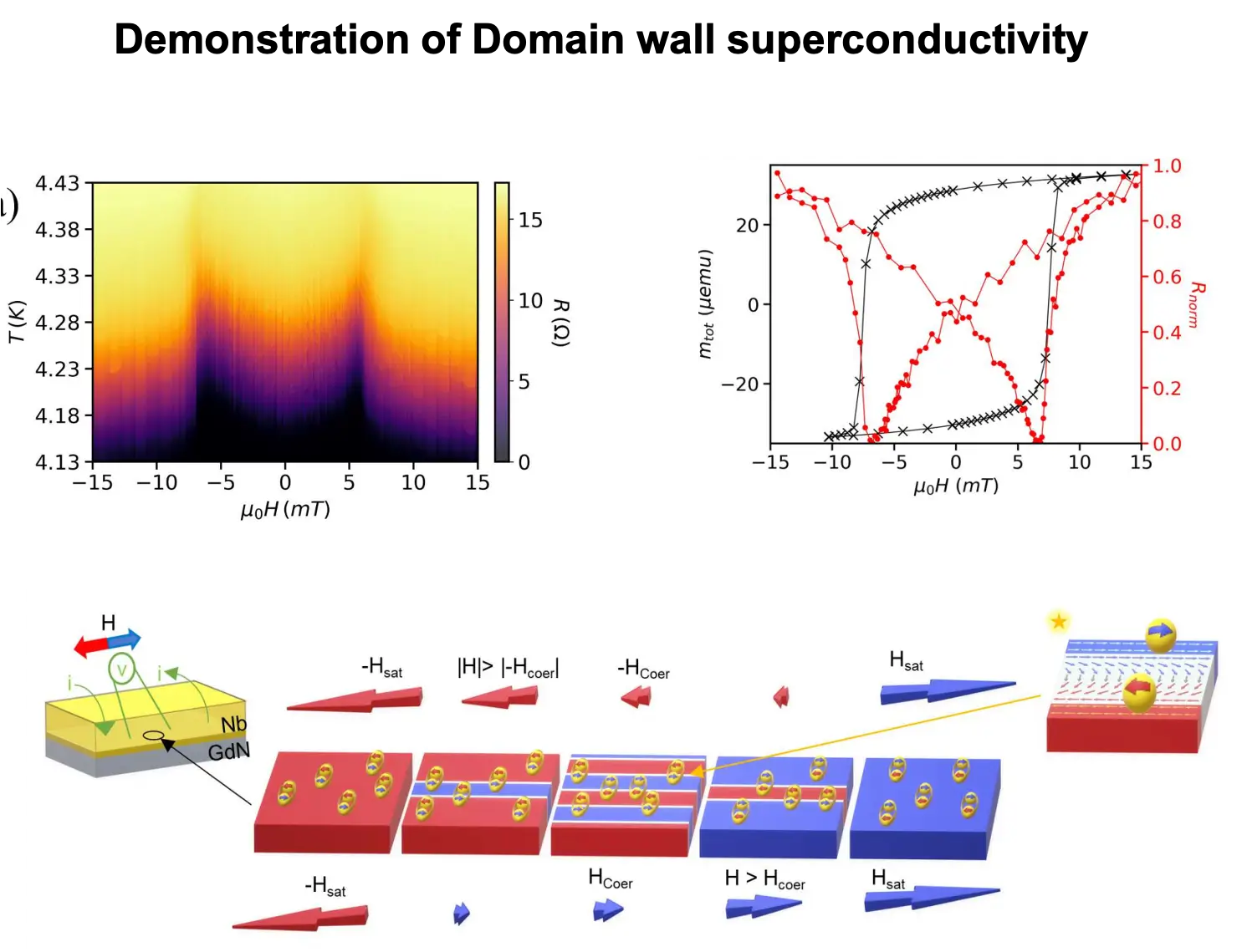
Domain wall superconductivity in GdN/Nb bilayers

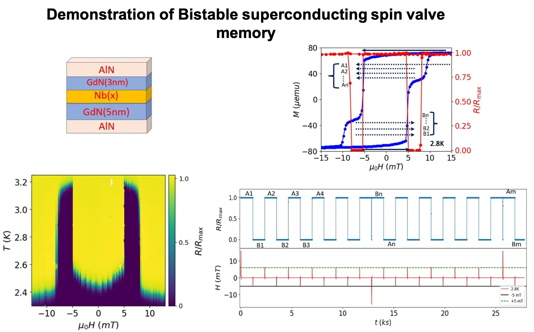
Superconducting exchange coupling driven memory device

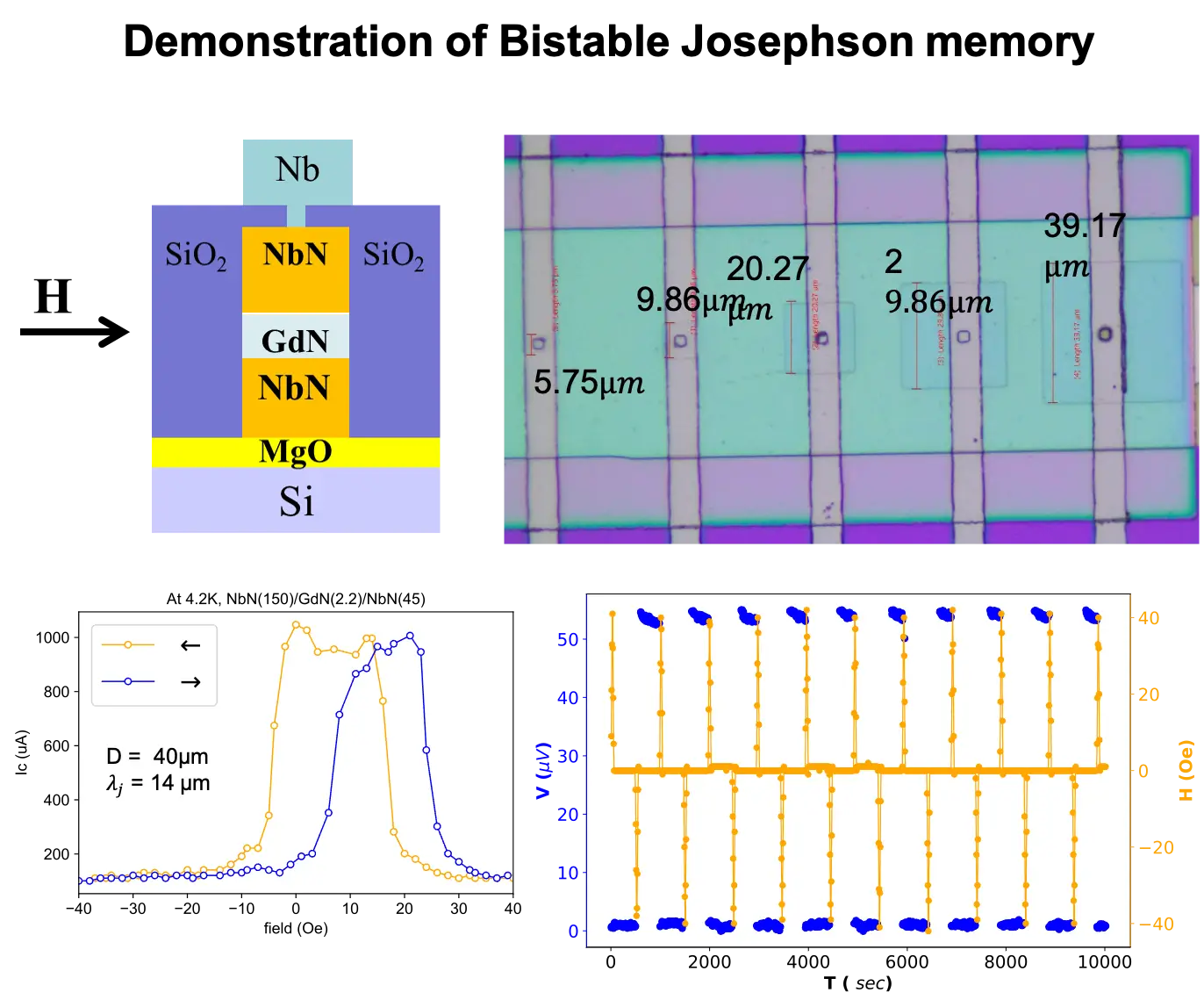
High frequency Josephson memory device at 4.2K

Faculty Details Aswani Yella

Associate Professor

Aswani Yella

Email: aswani[dot]yella[at]iitb[dot]ac[dot]in

Phone: (+91) (022) 2576 7619

Education: 

  • Ph.D. ­ Johannes Gutenberg University, Mainz, Germany, 2010 
  • M.Sc­ University of Hyderabad­2005
Teaching

Courses taught are 

UG courses: Thermodynamics of materials 

PG courses: Semiconductor photo electrochemistry and photocatalysis, Electrical and magnetic materials

Research profile

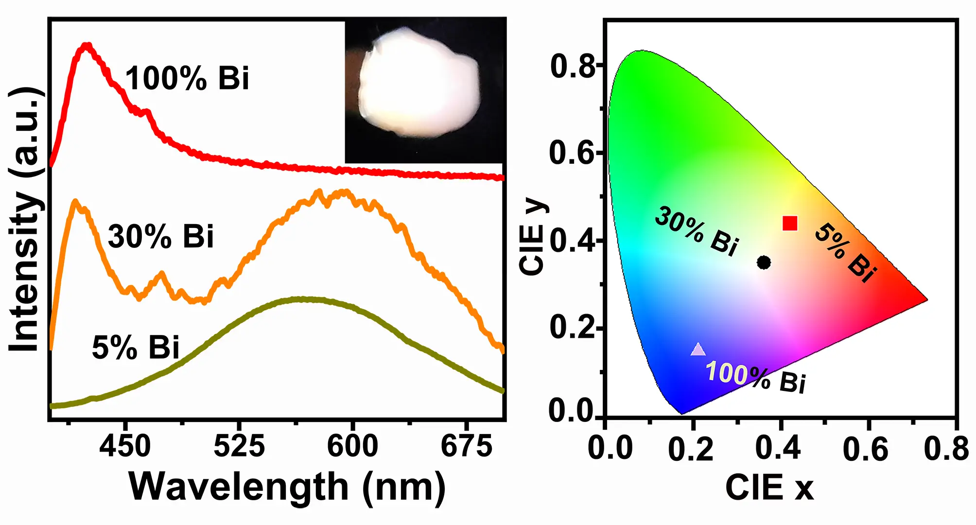
The group of optoelectronic materials and devices are interested in developing semiconductor materials for optoelectronic devices, in particular halide perovskite materials. Halide perovskites have many interesting properties like high absorption coefficient, large charge carrier diffusion lengths, ease of synthesis, etc. However their real life applications are hindered due to the moisture instability and the lead toxicity. The group found zero­ dimensional perovskites to transform to 3D perovskites in the presence of moisture and remain to be stable under moist conditions, which lead to the stable perovskite solar cells. Since the transformation takes place in the presence of humidity, these were found to be useful in making self powered humidity sensors. To address the lead toxicity, the group is focussed on developing lead free perovskites and found that Cs2AgInCl6 doped with Bi3+ to be emitting a broad range with white light emission, making it a single source white light emitter.

Research interest
  • Semiconductor Devices, 
  • Low cost photovoltaic devices, 
  • Photoelectrochemical cells

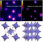
Zero dimensional perovskites to 3D perovskite transformation in the presence of moisture

Single source white light emitting Bismuth doped Cs2AgInCl6

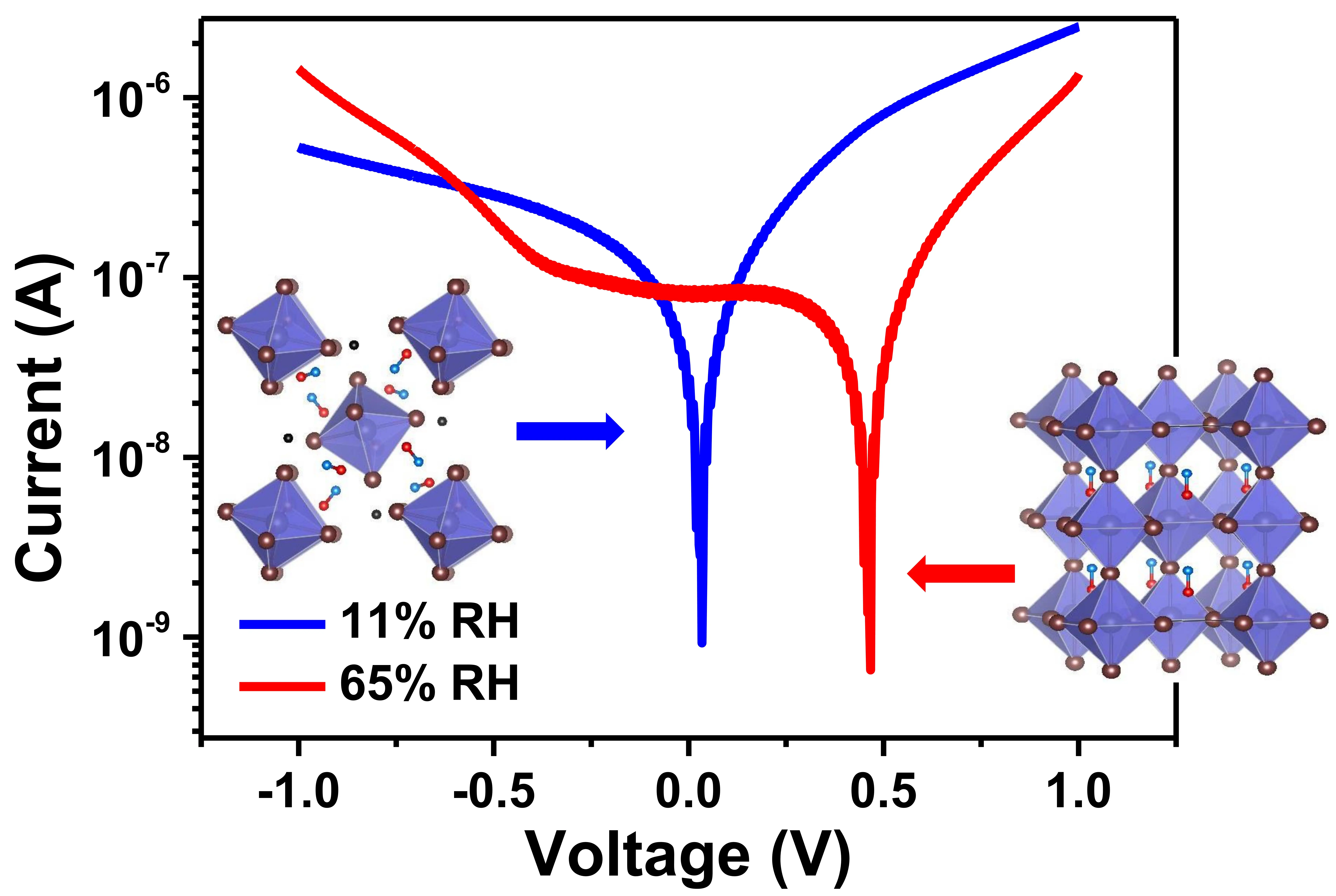
Moisture to electricity conversion using halide perovskites

References
  1. Moisture­Induced Ionovoltaic Electricity Generation by Manipulating Organic–Inorganic Hybrid Halide Perovskites Sumit Kumar Sharma, Monika Salesh, Mohanraj Subramaniam, Burhanuddin Attarwala, Aswani Yella ACS Energy Letters, 2023, 8,2259­2266 
  2. High performance acidic water electrooxidation catalysed by manganese–antimony oxides promoted by secondary metals Sibimol Luke, Manjunath Chatti, Douglas Mc Farlane, Aswani Yella, Rosalie Hocking, Alexandr Simonov EES Catalysis, 2023, 1, 730­741 
  3. Lead­Free Potassium Alloyed Cs2AgBiBr6: Tunable Optoelectronic Properties and Carrier­Lattice Interaction Vipinraj Sugathan, Jiban Kangsabnik, Aftab Alam, Aswani Yella Energy & Fuels, 2022, 36, 11100­ 11107

Faculty Details Aparna Singh

Associate Professor

Aparna Singh

Email: aparna_s[at]iitb[dot]ac[dot]in

Phone: (+91) (022) 2576 7605

Education:

  • BTech in Mtls. & Met.l Engg. IIT Kanpur, 2007 
  • PhD in Mtls. Sci. & Engg. MIT Cambridge, 2011
Teaching

Undergraduate Courses: Mechanics of Materials 

Postgraduate Courses: Fatigue of Materials, Tribology of Materials, Physical metallurgy and mechanical properties of steels

Research profile

Prof. Aparna Singh’s interest is in the development of novel materials with a combination of high strength, toughness and fatigue crack growth life. She is also interested in understanding processingmicrostructure­ processing links in steels and polymer composites. Her rigorous experimental work has shown many interesting deformation phenomena in epoxies and steels. She also has significant experience in probing causes of failures in rails and wheels. Multiple novel grades of steels have been developed in her group that have the potential to be used as rail/wheel materials. Novel varieties of hierarchical carbonfiber epoxy composites have also been developed in her lab that can find use in prosthetics , wind turbine blades and aeroplanes. She has also worked with industries like Renewsys and Shapoorji Pallonji.

Research interest
  • Rails and wheels Fracture and fatigue 
  • Physical and mechanical metallurgy of steels Polymer composites 
  • Reliability of PV modules

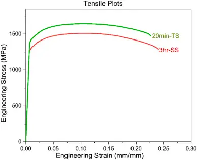
Enhanced tensile response in low carbon carbide free nano­bainitic steel

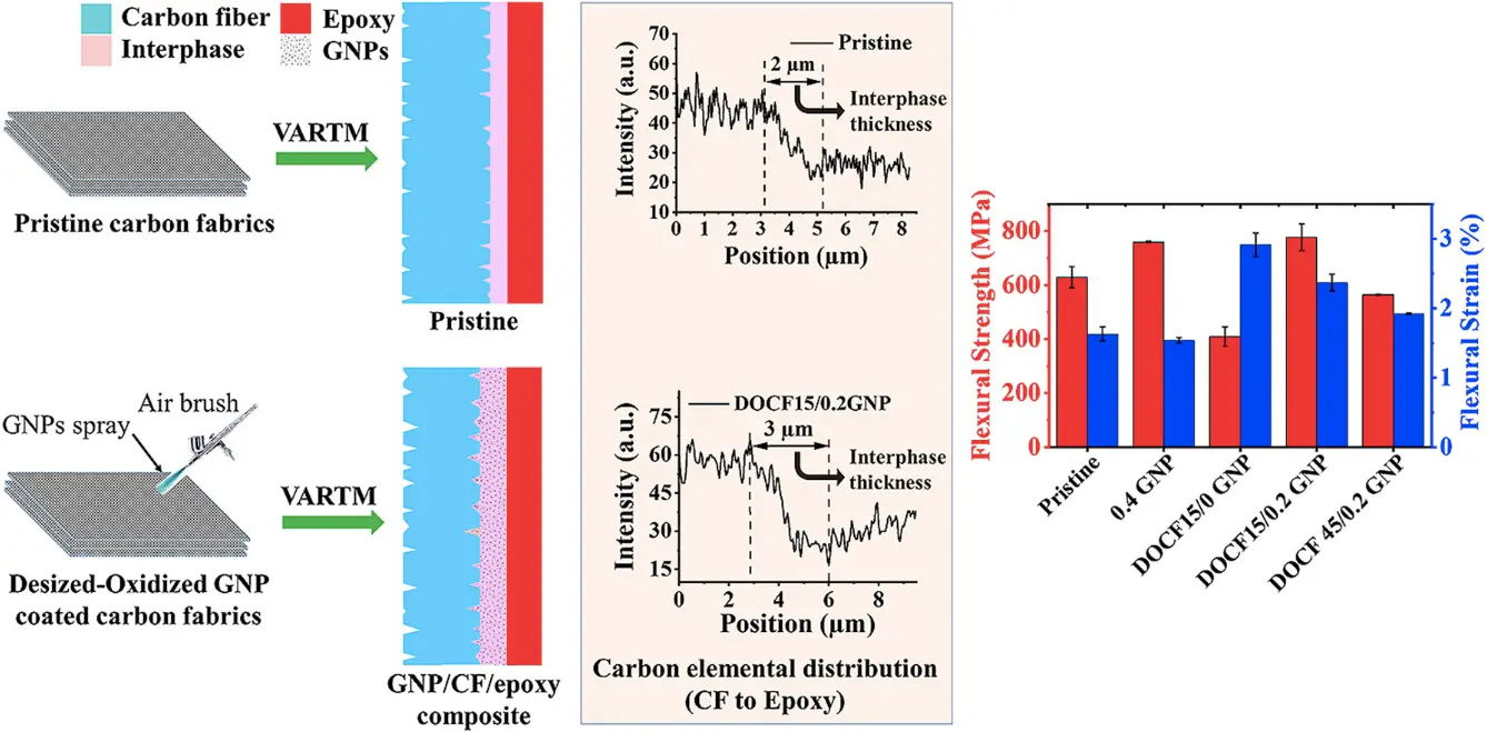
Enhancement of mechanical properties of carbon­fiber epoxy composites using graphene nano­platelets

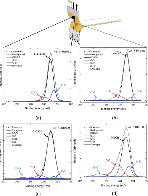
High resolution XPS spectra for peeled (a) BS18 in pristine condition, (b) EVA18 in pristine condition, (c) BS18 after DH aging and (d) EVA18 after DH aging

References
  1. A. Kumar, B. Blessto, A. Singh*, “Development of a low­carbon carbide­free nanostructured bainitic steel with extremely high strength and toughness.” Materials Science and Engineering A, 2023. 
  2. K. Mishra, A. Singh*, “Time­dependent degradation of highly cross­linked epoxy due to hygrothermal aging at three different temperatures.” Polymer Degradation and Stability, 2023 
  3. U. Desai, B. K. Sharma, A. Singh, A. Singh*, “A comparison of evolution of adhesion mechanisms and strength post damp­heat aging for a range of VA content in EVA encapsulant with photovoltaic backsheet.” Solar Energy, 2022. 
  4. S. Rathore, W. Leong, A. Singh*, “Mechanical properties estimation of 2D–3D mixed organic­inorganic perovskites based on methylammonium and phenylethyl­ammonium system using a combined experimental and first­principles approach.” Journal of Alloys and Compounds, 2023. 
  5. A. Srivastava, V. Gupta, C. Yerramali, A. Singh*, “Flexural strength enhancement in carbon­fiber epoxy composites through graphene nano­platelets coating on fibers.” Composites B: engineering, 2019. 
  6. K. Singh, A. Kumar, A. Singh*,” Effect of prior austenite grain size on the morphology of nano­bainitic steels.” Metallurgical and Materials Transactions A, 2018.
Subscribe to Semiconductor, Photovoltaics & Electronic Materials