

Institute Chair Professor
Rajiv O. Dusane
Email: rodusane[at]iitb[dot]ac[dot]in
Phone: (+91) (022) 2576 7633
Education:
- Ph.D. Physics, 1990, Univ. of Poona, Pune,
- M.Sc. Physics, Nagpur Univ 1984
Prof. Dusane has engaged students in thin films and semiconductor device processing courses over the last 20 or more years with special emphasis on the practical aspects. He also established the Thin Film lab for both UG and PG students. As his special interest he also took the communication course for the PG students.
Undergraduate course: Science and Technology of Thin Films
Postgraduate course: Materials and Processes for Semiconductor Device Manufacturing
Prof. Dusane has over the last 30 years carried out fundamental and applied research in the area of semiconductor thin films and devices, surface modification and plasma processing of various materials with a view to develop new processes and materials in thin film and nano structure form, capable for a variety of applications ranging from solar cells, thin film light emitting devices (TFLEDs), microelectronic devices, sensors and actuators (MEMS) and batteries. He has done pioneering work in the area of Hot Wire Chemical Vapor Deposition (HWCVD) process in this country. Several patents have resulted out of this work and some successful industrial collaborations have also been undertaken. Over these years he has established state of the art facilities for thin film deposition and characterization. Recent significant work from his group is the Silicon nanowirebased anode for Liion battery. The work carried out till now has demonstrated the capabilities of the Hot Wire process in diverse areas like Microelectronics, Biocompatible materials, surface functionalization and modification, barrier layers etc. This has given new directions to the applicability of the HWCVD process in the area of MEMS and sensors. Recently he has designed and developed a HWCVD multichamber cluster tool, the first of its kind in the country.
- Semiconductor thin films for optoelectronic devices,
- Photovoltaic devices,
- Energy storage
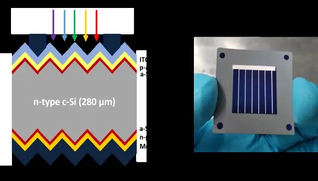
HIT solar cell on textured Silicon wafer architecture and fabricated cell
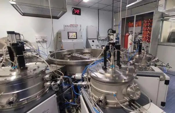
The newly developed HWCVD multichamber system
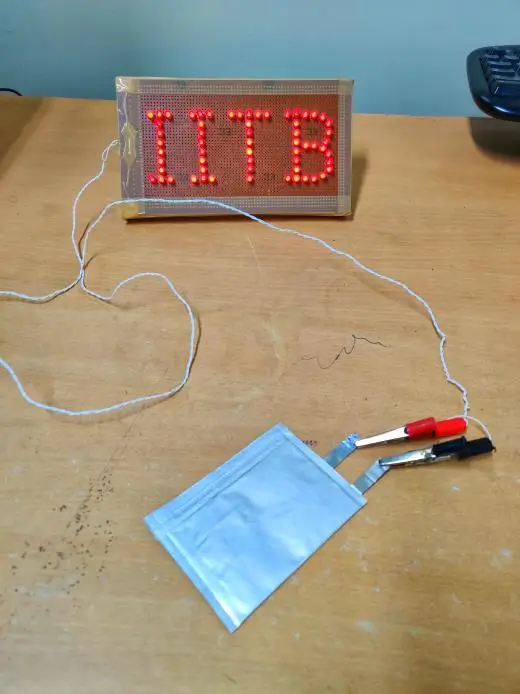
Silicon Nanowire Anode based Li ion pouch cell
- Rashmi Tripathi, V Chauhan, P Gandharapu, S Kobi, A Mukhopadhyay, R O Dusane. “Si Nanowires Grown on Cu Substrates via the HotWire Assisted Vapor–Liquid–Solid Method for Use as Anodes for LiIon Batteries”. ACS Applied Nano Materials (2022), 17767–17782.
- "Conformal Deposition of BxC in High Aspect Ratio Trenches for 3D neutron detectors", Gourav Kumar, Partha Karar, D S Patil, Arvind Singh, Anita Topkar, R O Dusane Thin Solid Films 720 (2021) 138521
- "Piezoresistive pressure sensor using nanocrystalline silicon thin film on flexible substrate", V Pandey, A Mandal, S Sisle, MP Gururajan, R O Dusane Sensors and Actuators A: Physical 316, 112372