

Assistant Professor
Abhinandan Gangopadhyay
Email: abhinandan[dot]g[at]iitb[dot]ac[dot]in
Phone: (+91) (022) 2576 7603
Education:
- PhD Materials Sc & Engg, Arizona State Univ, USA
- MTech Metallurgical Engg & Materials Sc, IIT Bombay, India
- BE Metallurgy & Materials, IIEST Shibpur, India
Prof. Gangopadhyay has taught undergraduate course on Mechanical Behaviour of Materials. He will be offering a comprehensive graduate level course on Transmission Electron microscopy.
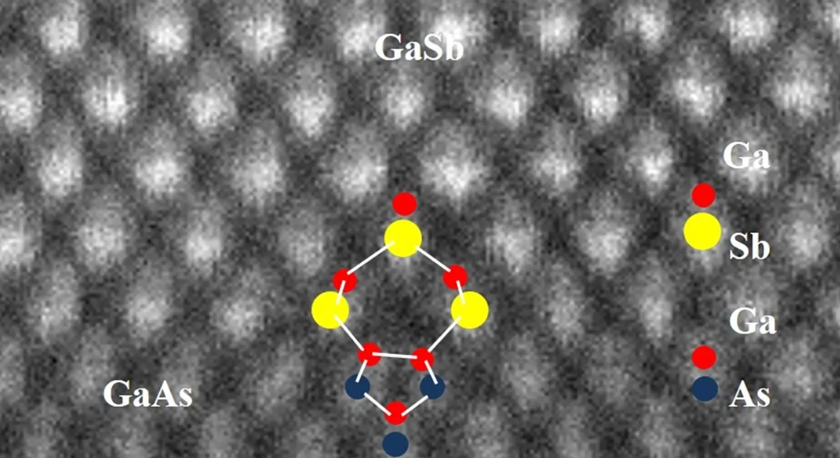
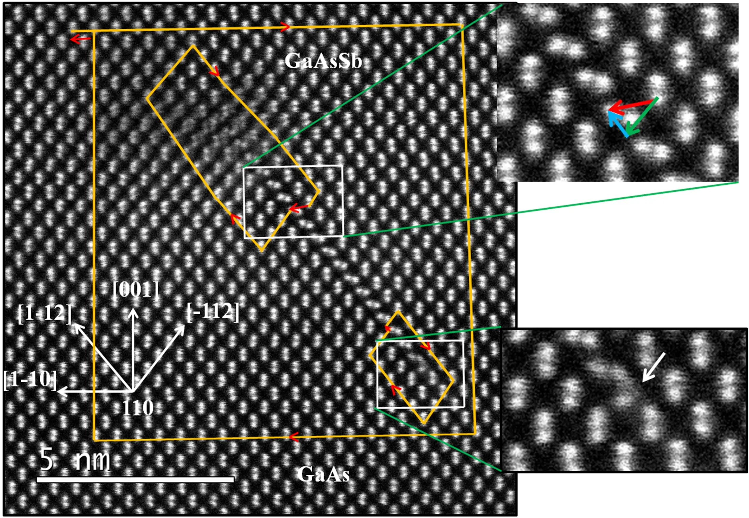
Prof. Abhinandan Gangopadhyay is interested in applying advanced electron microscopy techniques to study defects and interfaces in advanced functional and structural materials. He has previously studied the core structure of various interfacial defects such as dissociated 60° dislocation [1], Lomer dislocation [2], dissociated 90° dislocation [3] in GaAs(001)based heterostructures using highangle annulardarkfield (HAADF) mode of aberrationcorrected scanning transmission electron microscopy (ACSTEM). Prof. Gangopadhyay has also worked on STEMEDX characterization of grain boundary segregation in novel polycrystalline GaInP solar cells. As part of his recent industrial work experience, he has worked on nanometerscale characterization of stateoftheart semiconductor devices using focused ion beam (FIB) technique in conjunction with ACSTEM. His current research interests include segregation studies using STEM spectrum images and strain mapping using geometric phase analysis (GPA) and 4D STEM in advanced materials.
- Thin films of functional materials
- Pulsed Laser Deposition and Sputter Deposition
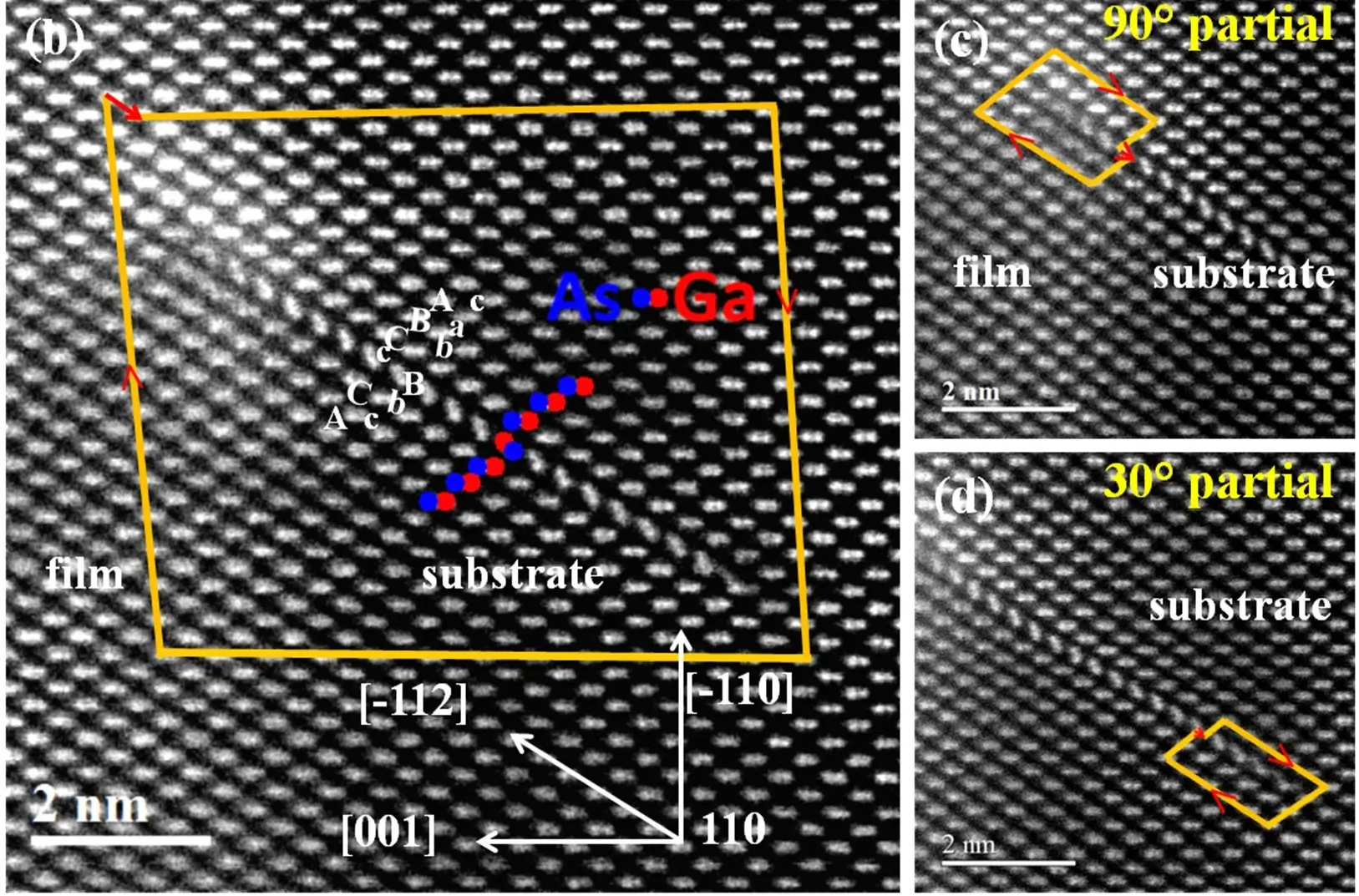
Aberrationcorrected HAADFSTEM images of dissociated 60 degree dislocation and its bounding partials located at GaAsSb/GaAs interface [1]
Aberrationcorrected HAADFSTEM image of a Lomer dislocation located at GaSb/GaAs interface [2]
Aberrationcorrected HAADFSTEM image of a dissociated 90 degree dislocation located at GaAsSb/GaAs interface [3]
- Gangopadhyay A, Maros A, Faleev N & Smith DJ. Atomic structure of dissociated 60° dislocations in GaAs/GaAs0.92Sb0.08/GaAs heterostructures. Scripta Materialia 2018;153:77–80.
- Gangopadhyay A, Rotter TJ, Balakrishnan G, Smith DJ. Atomicscale Structural Imaging of Interfacial Defects in GaAs(001)based Heterostructures. Microscopy and Microanalysis. 2021;27(S1):23562357.
- Gangopadhyay A, Zhang C, Maros A, Faleev, N, King RR, Honsberg CB & Smith, DJ Extended defects in GaAs/GaAs1xSbx/GaAs (001) heterostructures. Scripta Materialia 2023;225:115150.